
Shenzhen KHJ Technology Co., Ltd marketing@khj.cn 86-0755-28102935
Semiconductor package
Semiconductor packaging refers to a multi-process, so that the chip can meet the design requirements with independent electrical properties of the process. Packaging process is: from the wafer before the process of wafers through the wafer scribing process, was cut into small grains, and then cut the grains with a solid crystal machine in accordance with the requirements of fixed in the corresponding lead frame in the oven with nitrogen curing, and then use the wire bonding machine will be ultra-fine metal wire bonding pads to connect to the substrate pins, and constitutes the required circuitry; and then the use of molding machine will be independent of the wafer encapsulation with epoxy resin package To encapsulate the protection, this is the semiconductor packaging process. In the package after a series of operations, for finished product testing, and finally into the warehouse shipments.
Application of adhesive film in the packaging process
Semiconductor packaging process, packaging before the wafer cutting and packaging after the substrate cutting, is the entire packaging process is indispensable to the important process, cutting quality directly affects customer satisfaction and the company's benefits, cutting process affects the quality of a number of factors: cutter, cutting parameters, cutting blade, surfactant, coolant, film, etc., has been analyzed in front of the blade, process, cooling water in the cutting Application in cutting process.
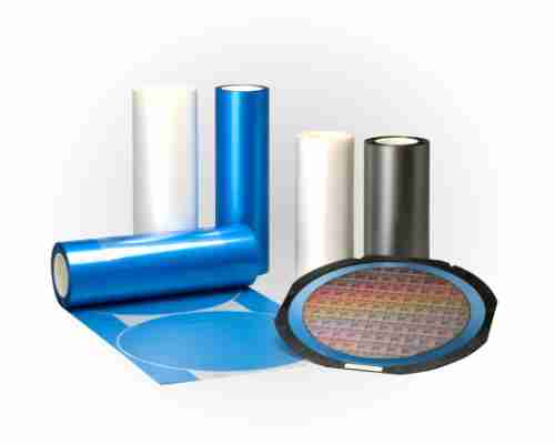
Blue film, also known as electronic grade adhesive tape, is mainly used for the protection of glass, aluminum plate, steel plate, because of its cost-effective and suitable for chip cutting, the back was introduced for chip cutting, and is now one of the mainstream wafer cutting tapes for domestic wafer cutting.
Common Abnormalities and Handling Methods
In the encapsulation cutting process, often encounter some cutting-related quality problems, caused by many reasons, improper selection of the film will also cause quality problems, common anomalies are: back chipping, flying material, wire drawing, residual adhesive, bubbles, staining. Here mainly from the perspective of the film to analyze the common abnormalities and the corresponding treatment.
Residual glue: 1.DB BLT deviation 2.bad conductivity cause: 1.film expiration 2.adhesive layer off prescription: 1.choose the right adhesive film
Fly hopper: 1. hit the knife 2. scratch the product cause: 1. big bubbles, dirty 2. low viscosity of the film prescription: 1. film in accordance with the norms of operation 2. extend the baking temperature and time.
Backfiring: 1. affect the stability of the product cause: 1. slight displacement of the chip 2. blade passivation prescription: 1. choose self-sharpening better blade 2. extend the baking time.
Excessive stickiness: 1.DB fetching difficulty 2.Impact on UPH cause: 1.Film baking temperature and time is too long 2.Film storage time is too long prescription: 1.Replacement of adhesive film with low viscosity 2.Reduction of baking time.